The major difference between PN junction and the Zener diode is that the PN junction diode allows current to pass only in the forward direction, whereas the Zener diode allows the current to flow both in the forward and the reversed direction. The other differences between the PN-junction and Zener diode are shown in the comparison chart.
The PN junction diode is used for rectification purpose because it allows the current to flow only in one direction. It is a type of switch which only allows the forward current to pass through it. On the other hand, the Zener diode allows both the forward and reverse current to pass through it. The Zener diode is used as a voltage regulator in the electronic circuit because it provides the constant voltage from the supply to the load whose voltage vary over sufficient range.
Content: PN Junction Vs Zener Diode
Comparison Chart
| Basis For Comparison | PN Junction Diode | Zener Diode |
|---|---|---|
| Definition | It is a semiconductor diode which conducts only in one direction, i.e., in forward direction. | The diode which allows the current to flow in both the direction i.e., forward and reverse, such type of diode is known as the Zener diode. |
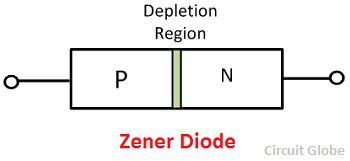
| Symbol | 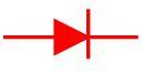 | 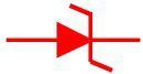 |
| Reverse Current Effect | Damage the junction. | Do not damage the junction. |
| Doping Level | Low | High |
| Breakdown | Occurs in higher voltage. | Occur in lower voltage. |
| Ohms Law | Obey | Do not obey. |
| Applications | For rectification | Voltage stabilizer, motor protection and wave shaping. |
Definition of PN Junction Diode
The PN junction diode is made up of semiconductor material. It is always conducted in one direction and hence used for rectification. The PN junction diode has two terminals namely anode and cathode. The current flows from anode to cathode.
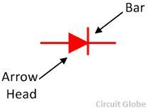
The PN junction diode conducts only when it is connected in forward biased. The symbolic representation of PN junction diode is shown in the figure above. The arrow head represents the positive potential, and the bar shows the negative potential of the diode.
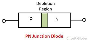
The PN junction diode has a P-type and N-type semiconductor material which is joined by the process of alloying. Thus, both the ends of the diode has different properties. The electrons are the majority charge carrier of the N-type material, and the holes are the majority charge carrier of the p-type semiconductor material. The region in which both the p-type and n-type material meets is known as the depletion region. This region does not have any free electrons because electrons and holes combine with each other in this region.
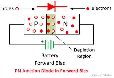
The depletion region is very thin, and it does not allow the current to flow through it. The PN junction starts conducting when the forward bias is applied across the junction. The forward bias means the P-type material is connected to the positive terminal of the battery and the N-type material is connected to the negative supply.
The forward biased creates the electric field which reduces the depletion region of the PN-junction diode. When the potential barrier is completely reduced, it creates the conducting path for the flow of current. Thus, large current starts flowing, and this current is called the forward current.
Definition of Zener Diode
The Zener diode is made up of silicon material. It is a special type of diode which operates in the breakdown region. It allows the current to flows both in the forward as well as in the reversed direction, when the Zener voltage is reached. The Zener diode is made by highly doped p-type and the n-type material, i.e. the concentration of ion is higher in the material.
When the reversed voltage is applied to the material, the depletion layer become reduces. Because of the thin depletion region, the concentration of the electric field is high. If the value of reverse voltage increases then the ions come out from the electrons and make the depletion region conductive. This breakdown of the depletion region is called the Zener breakdown and the voltage at which the breakdown occurs in known as the Zener voltage.
Key Differences Between PN-Junction and Zener Diode
The following are the key differences between the PN junction and Zener diode.
- The semiconductor which conducts only in one direction is known as the PN-junction diode. And the Zener diode is the silicon diode which is optimised to operate in the breakdown region.
- The reverse current flow through the diode damage the PN-junction diodes. The reverse current flows through the diode when it is connected in reverse biased. The reverse biasing means the p-type material is connected to the negative terminal of the supply and the n-type material is connected to the positive terminal of the supply. But the Zener diode allows the current to pass through both the direction.
- The doping level of the PN-junction diode is low as compared to Zener diode. The width of the depletion region depends on their doping level. If the doping level of the diode is high, their depletion region is low and vice versa.
- The breakdown in PN-junction diode occurs at high voltage level, whereas in PN-junction diode it occurs at low voltage levels. The breakdown is the phenomenon of making the depletion region conductive. The heavily doped diode has a low depletion region.
- The PN-junction obey the ohm’s law whereas Zener diode does not obey the ohms law. The ohms law said that the voltage applies across the diode is equal to the product of the current and resistance applied across the diodes.
- The PN-junction diode is mainly used for rectification purpose, whereas the Zener diode is used for providing the constant voltage to the load whose voltage vary.
Conclusion
The PN junction diode and the Zener diode both are made up of semiconductor material. They are differentiated by their property of current conduction.The PN junction is lightly doped and having large depletion region which is only eliminated by forward biasing. And the Zener diode is heavily doped and has thin depletion which makes their conduction easy even in the low biasing.
What about the noise they generate when reverse biased? Both Transistor and Zeners produce it, but Zeners seem way more prominent, due to size of junction/doping?