A Flip Flop is a bi-stable device. There are three classes of flip flops they are known as Latches, pulse-triggered flip-flop, Edge- triggered flip flop. In this set word means that the output of the circuit is equal to 1 and the word reset means that the output is 0.
There are two types of flip flop one is RS Flip Flop and JK Flip Flop. In this article, RS Flip Flop is explained in detail.
Contents:
The RS Flip Flop is considered as one of the most basic sequential logic circuits. The Flip Flop is a one-bit memory bi-stable device.
It has two inputs, one is called “SET” which will set the device (output = 1) and is labelled S and another is known as “RESET” which will reset the device (output = 0) labelled as R. The RS stands for SET/RESET.
The flip-flop is reset back to its original state with the help of RESET input and the output is Q that will be either at logic level “1” or logic”0”. It depends upon the set/reset condition of the flip-flop. Flip flop word means that it can be “FLIPPED” into one logic state or “FLOPPED” back into another.
The basic NAND gate RS Flip Flop circuit is used to store the data and thus provides feedback from both of its outputs again back to its inputs. The RS Flip Flop actually has three inputs, SET, RESET and its current output Q relating to its current state.
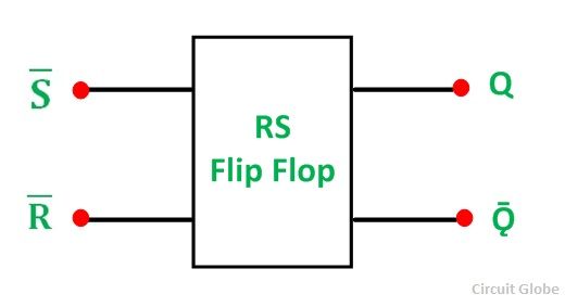
The symbol of the RS Flip-Flop is shown below:
The NAND Gate RS Flip Flop
A pair of cross-coupled 2 unit NAND gates is the simplest way to make any basic one-bit set/reset RS Flip Flop. It forms Set/Reset bi-stable or an active LOW RS NAND gate latch. The feedback is fed from each output to one of the other NAND gate input.
The device consists of two inputs; one is known as SET, (S) and the other is called as RESET, (R).
The two outputs are Q and Q bar as shown in the figure below:
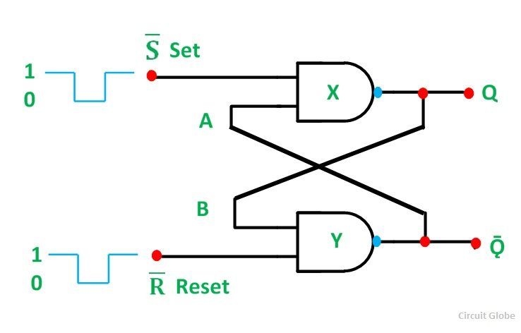
The Set State
Considering the above circuit. If the input R is at logic level “0” (R = 0) and input S is at the logic “1” (S = 1), the NAND gate Y has, at least, one of its inputs at a logic “0”. Therefore, its output Q must be at a logic level “1” (NAND gate principles). The Output (Q) is fed back to the input “A”. Both the inputs of the NAND gates X are at logic “1”, and therefore, its output Q must be at the logic level”0”.
The reset input R changes its state, and goes HIGH to logic “1” with S constant at logic “1”. The NAND gate Y input are now (R = 1) and (B = 0). The output at Q remains at HIGH or at logic level “1” as one of its inputs is still at logic level “0”.
As a result, there is no change in state. Therefore, the flip-flop circuit is said to be “LATCHED” or “SET” with Q = 1 and Ǭ = 0.
The Reset State
In this second stable state, Q is at logic level ‘0” and its inverse output Q is at logic level “1”. And is given by (R = 1) and (S = 0). As gate X has one of its inputs at a logic “0” its output Q must equal logic level “1”. (According to the NAND gate principle). The output Q is fed to input B, so both the inputs to NAND gate Y are at logic “1”., therefore, Q = 0.
If the set input S now changes the state to logic “1” with the input R remaining at logic “1”, the output Q still remains LOW at logic level “0”. And there is no change in the state.
Therefore, the flip-flop circuits “RESET” state has been latched.
The truth table of the Set/Reset is given below:
| State | S | R | Q | Ǭ | Description |
|---|---|---|---|---|---|
| SET | 1 | 0 | 1 | 0 | Set Q >>1 |
| 1 | 1 | 1 | 0 | No Change | |
| RESET | 0 | 1 | 0 | 1 | Reset Q >>0 |
| 1 | 1 | 0 | 1 | No Change | |
| INVALID | 0 | 0 | 0 | 1 | Memory with Q = 0 |
| 0 | 0 | 1 | 0 | Memory with Q = 1 |
From the truth table, it is clear that when both the inputs S = 1 and R =1 the outputs Q, and Ǭ can be at either logic level ‘1’ or “0” depending upon the state of the inputs.
When the input state R = 0 and S = 0 is an invalid condition and must be avoided because this will give both outputs Q and Ǭ at logic level “1” at the same time and the necessary condition is that Q to be the inverse of Ǭ.
The flip-flop goes to an unstable state as both the output goes LOW. This unstable condition arises when the LOW input is switched to HIGH. The flip-flop switches to one state or the other and any one output of the flip-flop switches faster than the other. This unstable condition is known as Meta- stable state.
The bistable RS flip flop is activated or set at logic “1” applied to its S input and deactivated or reset by a logic “1” applied to R. The RS flip-flop is said to be in an invalid condition if both the set and reset inputs are activated simultaneously.
The NOR Gate RS Flip Flop
The circuit diagram of the NOR gate flip-flop is shown in the figure below:
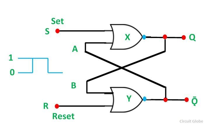 A simple one bit RS Flip Flops are made by using two cross-coupled NOR gates connected in the same configuration. The circuit will work similar to the NAND gate circuit.
The truth table of the NOR gate RS Flip Flop is shown below:
| S | R | Q | Ǭ |
|---|---|---|---|
| 0 | 0 | No Change | No Change |
| 0 | 1 | 0 | 1 |
| 1 | 0 | 1 | 0 |
| 1 | 1 | 0 | 0 |
The inputs are active HIGH and the invalid condition exists when both its inputs are at logic level ‘1’.
Nice … thanks for giving this information… about.rs…
THANK U.
thank u
nicely explained . its very useful for me as being AMIE student
Very nice and helpful content.
Thank you
very educational thank you
It was really nice.
Nice statement of the flip flop
Good article for digital electronics students!
Thanks
GREAT ARTICLE
Very nice 👌
Very nice 👍
GREAT JOB. PERFECTLY UNDERSTOOD