The JK Flip Flop is the most widely used flip flop. It is considered to be a universal flip-flop circuit. The sequential operation of the JK Flip Flop is the same as for the RS flip-flop with the same SET and RESET input.
The difference is that the JK Flip Flop does not the invalid input states of the RS Latch (when S and R are both 1). The JK Flip Flop name has been kept on the inventor name of the circuit known as Jack Kilby.
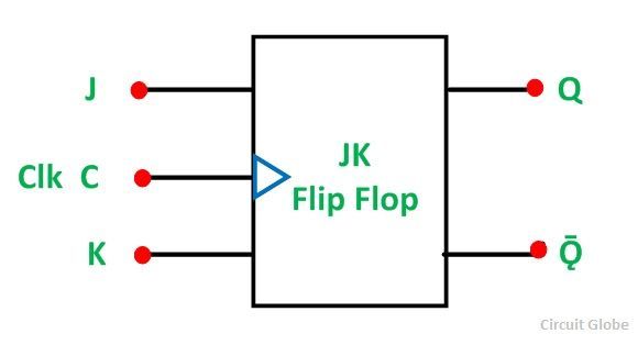
The basic symbol of the JK Flip Flop is shown below:
The basic NAND gate RS flip-flop suffers from two main problems.
- Firstly, the condition when S = 0 and R = 0 should be avoided.
- Secondly, if the state of S or R changes its state while the input which is enabled is high, the correct latching action does not occur.
Thus to overcome these two problems of the RS Flip-Flop, the JK Flip Flop was designed.
The JK Flip Flop is basically a gated RS flip flop with the addition of the clock input circuitry. When both the inputs S and R are equal to logic “1”, the invalid condition takes place.
Thus, to prevent this invalid condition, a clock circuit is introduced. The JK Flip Flop has four possible input combinations because of the addition of the clocked input. The four inputs are “logic 1”, ‘logic 0”. “No change’ and “Toggle”.
The circuit diagram of the JK Flip Flop is shown in the figure below:
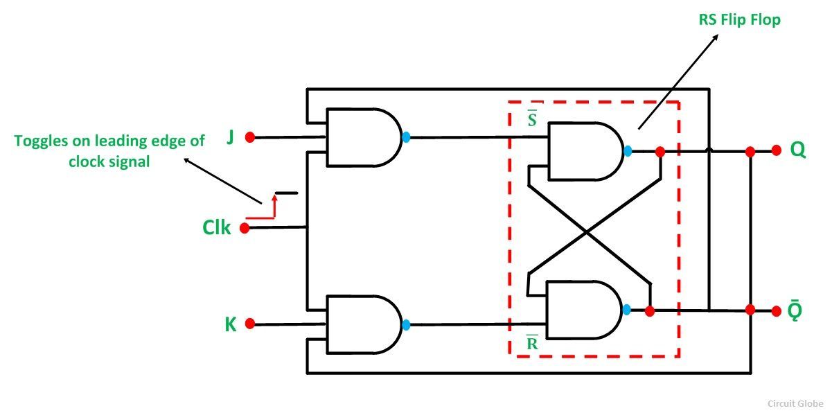
The S and R inputs of the RS bistable have been replaced by the two inputs called the J and K input respectively.
Here J = S and K = R. The two-input AND gates of the RS flip-flop is replaced by the two 3 inputs NAND gates with the third input of each gate connected to the outputs at Q and Ǭ. This cross-coupling of the RS Flip-Flop is used to produce toggle action. As the two inputs are interlocked.
If the circuit is in the “SET” condition, the J input is inhibited by the status 0 of Q through the lower NAND gate. Similarly, the input K is inhibited by 0 status of Q through the upper NAND gate in the “RESET” condition.
When both J and K are at logic “1”, the JK Flip Flop toggle.
The Truth Table of the JK Flip Flop is shown below.
| J | K | Q | Ǭ | Description | |
|---|---|---|---|---|---|
| Same as for the RS Latch | 0 | 0 | 0 | 0 | Memory No Change |
| 0 | 0 | 0 | 1 | ||
| 0 | 1 | 1 | 0 | Reset Q >> 0 | |
| 0 | 1 | 0 | 1 | ||
| 1 | 0 | 0 | 1 | Set Q >> 1 | |
| 1 | 0 | 1 | 0 | ||
| Toggle | 1 | 1 | 0 | 1 | Toggle |
| 1 | 1 | 1 | 0 |
JK Flip Flop is similar to RS flip flop with the feedback which enables only one of its input terminals. It eliminates the invalid condition which arises in the RS flip flop and put the input terminal either to set or reset condition one at a time.
When both the J and K inputs are at logic “1” at the same time and the clock input is pulsed HIGH, the circuit toggle from its SET state to a RESET or visa versa. When both the terminals are HIGH the JK flip-flop acts as a T type toggle flip-flop.
JK flip-flop has a drawback of timing problem known as “RACE”. The condition of RACE arises if the output Q changes its state before the timing pulse of the clock input has time to go in OFF state.
The timing pulse period (T) should be kept as short as possible to avoid the problem of timing.
This condition is not possible always thus a much-improved flip-flop named Master Salve JK Flip Flop was developed. This eliminates all the timing problems by using two RS flip-flop connected in series. One is for the “MASTER “ circuit, which triggers on the leading edge of the clock pulse. The other is called the “SLAVE” circuit, which triggers when the clock pulse is at the falling edge.