When a p-type semiconductor is suitably joined to an n-type semiconductor, the contact surface so formed is called p-n Junction. All the semiconductor devices contain one or more p n junction. The p-n junction is in effect, the control element for semiconductor devices.
Formation of p-n Junction
In actual practice, the PN junction is not formed just by bringing a p-type semiconductor block near to an n-type semiconductor block. Actually, p n junction is fabricated by special technique, namely growing, alloying and diffusing methods.
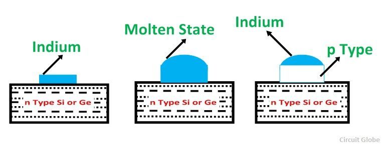
The most common method of making p n junction is called Alloying. An alloyed junction is made from an n-type of semiconductor made of germanium or silicon, by melting of the pellet of trivalent indium placed on either side. The whole arrangement or system is heated to about 500 degree Celsius. The indium is absorbed into the germanium or silicon to produce a p region and hence a p n junction is formed as shown in the figure below.
Another method to form a p n Junction is known as Diffusion. In this process, the semiconductor wafers of one conductivity either p-type or n-type are placed in a vessel that contains an oxide of the impurity to be added. The combination is passed slowly through a furnace with a controlled temperature of 800⁰C to 1200⁰C depending upon the type of junction. At such a high temperature, a gas of impurity atoms diffuses into the semiconductor material and forms a thin layer of opposite conductivity. Thus, resulting in the formation of the p n junction.
Properties of p n Junction
For understanding the property of a PN Junction, let us consider two types of extrinsic semiconductors. One is p-type, and the other one is of n-type as shown in the figure below.
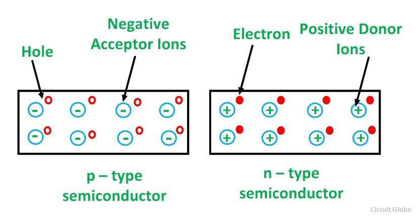
The p-type semiconductor is having negative acceptor ions and positively charged holes. Whereas, the n-type semiconductor is having positive donor ions and negatively charged electrons. When the two pieces are joined together and suitably treated, they form a pn Junction. The electron-hole recombination takes place a soon as the p n Junction is formed due to the reason that some of the electrons from n-type material diffuse over to the p-type material with the holes available in the valence band.
Similarly, hole-electron combination takes place when the holes from p-type material diffuse over to the n-type material, and the electron is available in the conduction band. This process of combination is known as Diffusion.
In diffusion, some of the free electrons move across the junction from n-type to p-type leaving behind positive donor ions. This establishes the positive charge on the n side of the junction. Simultaneously, the free electrons which cross the junction recombine with the hole of p-type and uncover some of the negative acceptor ions as shown in the figure below.
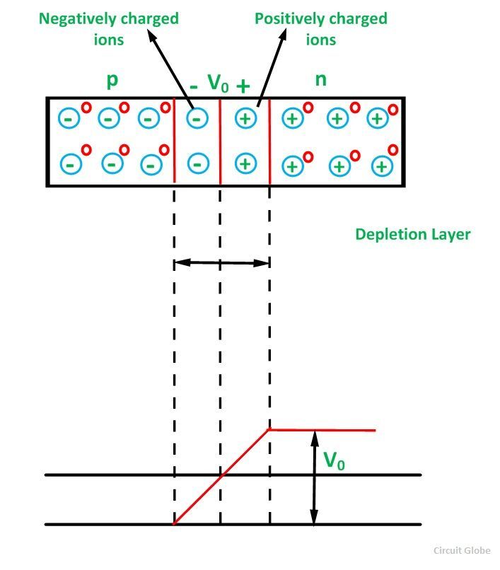
A negative charge is established on the p side of the junction. This process of diffusion continues until and unless a sufficient number of impurity ions in the form of donor and acceptor impurity are uncovered and a potential difference of nearly 0.3 V is developed in case the p n junction is formed by the Germanium material. Similarly, the potential difference of 0.7 V has to develop if the p n junction is formed by the silicon semiconductor material.
Once all this happens further diffusion is prevented and the potential difference created across the junction acts as a barrier which prevents further movement of electrons and holes. The positive charge on n side repels holes on p side and a negative charge on n side repels free electron of p side. This barrier is known as a Potential Barrier or Junction Barrier VO.
Potential Barrier
A potential difference built across the p n Junction, which restricts the further movement of charge carriers across the junction, is known as Potential Barriers.
Depletion Layer
A layer is formed on both the side of the junction. This layer is depleted of free electrons and holes. A region around the junction from which the charge carriers are depleted is called a Depletion Layer.