A p n junction is said to be operating under the biasing condition if it is connected across an electric supply. The potential difference across the p n junction can be applied in two ways, namely Forward Biasing and Reverse Biasing.
When the positive terminal of a DC source or battery is connected to p-type, and the negative terminal to the n-type semiconductor of a pn junction as shown in the figure below, the junction is said to be in Forward Biased condition.
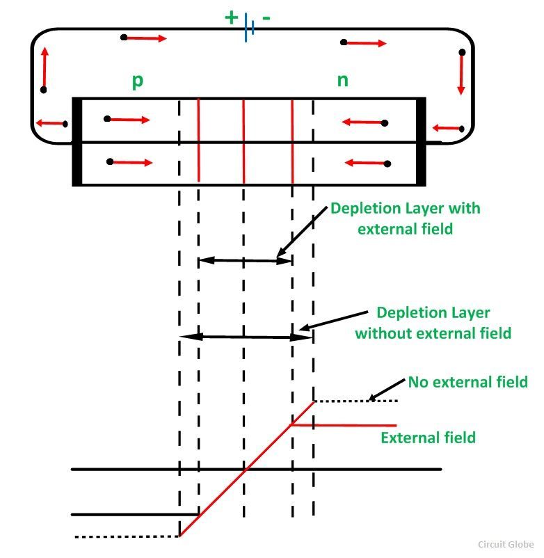
The applied forward potential establishes an electric field which reduces the field created due to the potential barrier. Thus, the potential barrier at the junction is reduced. A forward voltage is sufficient to eliminate the barrier because the voltage of the potential barrier is very small. (0.7 V for silicon and 0.3 V for germanium).
Once the potential barrier is eliminated, a conducting path is established for the flow of current. Thus, a large current starts flowing through the junction. This current is called Forward Current.
The external voltage applied to a p n junction that cancels the potential barrier to constitute an easy flow of current through it is called Forward Biasing.
When the p n junction is forward biased the following points are important. They are as follows:
- The junction potential barrier is reduced and at some forward voltage, it is eliminated.
- The junction offers low resistance, known as Forward Resistance (Rf) to the flow of current through it.
- The magnitude of the flow of the current through the circuit depends upon the applied forward voltage.
This is all about forward bias p n Junction.