One of the major difference between the forward and the reverse biasing is that in forward biasing the positive terminal of the battery is connected to the p-type semiconductor material and the negative terminal is connected to the n-type semiconductor material. Whereas in reverse bias the n-type material is connected to the positive terminal of the supply and the p-type material is connected to the negative terminal of the battery. The forward and reverse biasing is differentiated below in the comparison chart.
Biasing means the electrical supply or potential difference is connected to the semiconductor device. The potential difference is of two types namely – forward bias and the reverse bias.
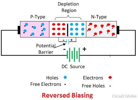
The forward bias reduces the potential barrier of the diode and establishes the easy path for the flow of current. While in reverse bias the potential difference increases the strength of the barrier which prevents the charge carrier to move across the junction. The reverse bias provides the high resistive path to the flow of current, and hence no current flows through the circuit.
Content: Forward Biasing Vs Reverse Biasing
Comparison Chart
| Basis for Comparison | Forward Biasing | Reverse Biasing |
|---|---|---|
| Definition | The external voltage which is applied across the PN-diode for reducing the potential barrier to constitutes the easy flow of current through it is called forward bias. | The external voltage which is applied to the PN junction for strengthening the potential barrier and prevents the flow of current through it is called reverse bias. |
| Symbol | 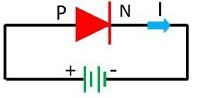 | 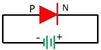 |
| Connection | The positive terminal of the battery is connected to the P-type semiconductor of the device and the negative terminal is connected to N-type semiconductor | The negative terminal of the battery is connected to the P-region and the positive terminal of the battery is connected to N-type semiconductor. |
| Barrier Potential | Reduces | Strengthen |
| Voltage | The voltage of an anode is greater than cathode. | The voltage of cathode is greater than an anode. |
| Forward Current | Large | Small |
| Depletion layer | Thin | Thick |
| Resistance | Low | High |
| Current Flow | Allows | Prevents |
| Magnitude of Current | Depends on forward voltage. | Zero |
| Operate | Conductor | Insulator |
Definition of Forward Biasing
In forward biasing the external voltage is applied across the PN-junction diode. This voltage cancels the potential barrier and provides the low resistance path to the flow of current. The forward bias means the positive region is connected to the p-terminal of the supply and the negative region is connected to the n-type of the device.
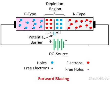
The potential barrier voltage is very small (nearly 0.7 V for silicon and 0.3 V for germanium junction) hence very few amount of voltage is required for the complete elimination of the barrier. The complete elimination of the barrier constitutes the low resistance path for the flow of current. Thus, the current starts flowing through the junction. This current is called forward current.
Definition of Reverse Biasing
In reversed bias the negative region is connected to the positive terminal of the battery and the positive region is connected to the negative terminal. The reverse potential increases the strength of the potential barrier. The potential barrier resists the flow of charge carrier across the junction. It creates a high resistive path in which no current flows through the circuit.
Key Differences between Forward and Reverse Biasing
- The forward bias reduces the strength of the potential barrier due to which the current easily move across the junction whereas reverse bias strengthens the potential barrier and obstruct the flow of charge carrier.
- In forward biasing the positive terminal of the battery is connected to the p-region and the negative terminal is connected to the n-type material while in reverse bias the positive terminal of the supply is connected to the n- type material and the negative terminal is connected to the p-type material of the device.
- The forward bias set up the electric field across the potential which reduces the strength of the potential barrier whereas the reverse bias increases the strength of the potential barrier.
- Note -The potential barrier is the layer between the PN junction diode which restrict the movement of electrons across the junction.
- In forward biasing the voltage of the anode is greater than the cathode whereas in reverse bias the voltage of the cathode is greater than the anode.
- The forward bias has large forward current while the reverse bias has very small forward current.
- Note – The current in the diode when flow in the forward direction is called forward current.
- The depletion layer of the diode is very thin in forward biasing and thick in reverse bias.
- Note – The depletion layer is the region around the junction in which the free charge carriers are depleted.
- The Forward bias decreases the resistance of the diode whereas the reversed bias increases the resistance of the diode.
- In forward biasing the current is easily flowing through the circuit whereas reverse bias does not allow the current to flow through it.
- In forward biasing the magnitude of the current depends on the forward voltage whereas in reverse bias the magnitude of the current is very small or negligible.
- In forward biasing the device operates as a conductor whereas in reverse bias the device act as an insulator.
The forward voltage of the silicon diode is 0.7 volts, and the forward voltage of the germanium is 0.3 volts.
Very clear and to the point and it helped me a lot to understand about p n Junction and Zener diode thanks a lot…
Nice one Thank you for the notes !!!
Nice notes it’s simple to understand
thank you
your god dam write..good one
Thanks a lot, its understandable
It’s easy to comprehend, helps a lot
Thank u so much
Thanks it is informative for us
Thanks .this is informative for us