Definition: The transistor is a semiconductor device which transfers a weak signal from low resistance circuit to high resistance circuit. The words trans mean transfer property and istor mean resistance property offered to the junctions. In other words, it is a switching device which regulates and amplify the electrical signal likes voltage or current.
The transistor consists two PN diode connected back to back. It has three terminals namely emitter, base and collector. The base is the middle section which is made up of thin layers. The right part of the diode is called emitter diode and the left part is called collector-base diode. These names are given as per the common terminal of the transistor. The emitter based junction of the transistor is connected to forward biased and the collector-base junction is connected in reverse bias which offers a high resistance.
Transistor Symbols
There are two types of transistor, namely NPN transistor and PNP transistor. The transistor which has two blocks of n-type semiconductor material and one block of P-type semiconductor material is known as NPN transistor. Similarly, if the material has one layer of N-type material and two layers of P-type material then it is called PNP transistor. The symbol of NPN and PNP is shown in the figure below.

The arrow in the symbol indicates the direction of flow of conventional current in the emitter with forward biasing applied to the emitter-base junction. The only difference between the NPN and PNP transistor is in the direction of the current.
Transistor Terminals
The transistor has three terminals namely, emitter, collector and base. The terminals of the diode are explained below in details.
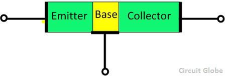
Emitter – The section that supplies the large section of majority charge carrier is called emitter. The emitter is alway connected in forward biased with respect to the base so that it supplies the majority charge carrier to the base. The emitter-base junction injects a large amount of majority charge carrier into the base because it is heavily doped and moderate in size.
Collector – The section which collects the major portion of the majority charge carrier supplied by the emitter is called a collector. The collector-base junction is always in reverse bias. Its main function is to remove the majority charges from its junction with the base. The collector section of the transistor is moderately doped, but larger in size so that it can collect most of the charge carrier supplied by the emitter.
Base – The middle section of the transistor is known as the base. The base forms two circuits, the input circuit with the emitter and the output circuit with the collector. The emitter-base circuit is in forward biased and offered the low resistance to the circuit. The collector-base junction is in reverse bias and offers the higher resistance to the circuit. The base of the transistor is lightly doped and very thin due to which it offers the majority charge carrier to the base.
Working of Transistor
Usually, silicon is used for making the transistor because of their high voltage rating, greater current and less temperature sensitivity. The emitter-base section kept in forward biased constitutes the base current which flows through the base region. The magnitude of the base current is very small. The base current causes the electrons to move into the collector region or create a hole in the base region.
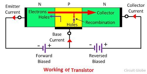
The base of the transistor is very thin and lightly doped because of which it has less number of electrons as compared to the emitter. The few electrons of the emitter are combined with the hole of the base region and the remaining electrons are moved towards the collector region and constitute the collector current. Thus we can say that the large collector current is obtained by varying the base region.
Transistor Operating Conditions
When the emitter junction is in forward biased and the collector junction is in reverse bias, then it is said to be in the active region. The transistor has two junctions which can be biased in different ways. The different working conduction of the transistor is shown in the table below.
| Condition | Emitter Junction (EB) | Collector Junction (CB) | Region of Operation |
|---|---|---|---|
| FR | Forward-biased | Reversed-biased | Active |
| FF | Forward-biased | Forward-biased | Saturation |
| RR | Reversed-biased | Reversed-biased | Cut-off |
| RF | Reversed-biased | Forward-biased | Inverted |
FR – In this case, the emitter-base junction is connected in forward biased and the collector-base junction is connected in reverse biased. The transistor is in the active region and the collector current is depend on the emitter current. The transistor, which operates in this region is used for amplification.
FF – In this condition, both the junction is in forward biased. The transistor is in saturation and the collector current becomes independent of the base current. The transistors act like a closed switch.
RR – Both the current are in reverse biased. The emitter does not supply the majority charge carrier to the base and carriers current are not collected by the collector. Thus the transistors act like a closed switch.
RF – The emitter-base junction is in reverse bias and the collector-base junction is kept in forward biased. As the collector is lightly doped as compared to the emitter junction it does not supply the majority charge carrier to the base. Hence poor transistor action is achieved.
I always wanted to clear my concepts about transistors but was scared about the complexity but this article made my day. Thanks for this awesome post.
Awesome notes ever 👍
Really awesome I was able to understand every topic easily because of these notes thanks a lot.
Your language is very easy; it’s helpful to clear the concept of transistors, really amazing
Just checked this out today. These notes are well prepared and informative. You’re amazing
Excellent contents and graphics.
Thank you for such a brilliant explanation
Best explaination
Great explanation about Transistors
I loved it.
Awesome, well organized notes 👍👍