A p n junction is known as a Semiconductor Diode. The p n junction is used for the purpose of rectification as it conducts only in one direction. It is also known as crystal diode as it is made of a crystal-like Silicon or Germanium. The symbol of the semiconductor diode is shown below.
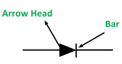 It has two terminals. It conducts only when it is forward biased. This means when the terminal connected with the arrowhead is at a higher potential than the terminal connected to the bar as shown in the above figure. When the semiconductor diode is reversed biased, practically it does not conduct any current through it.
Volt-Ampere Characteristics of a Semiconductor Diode
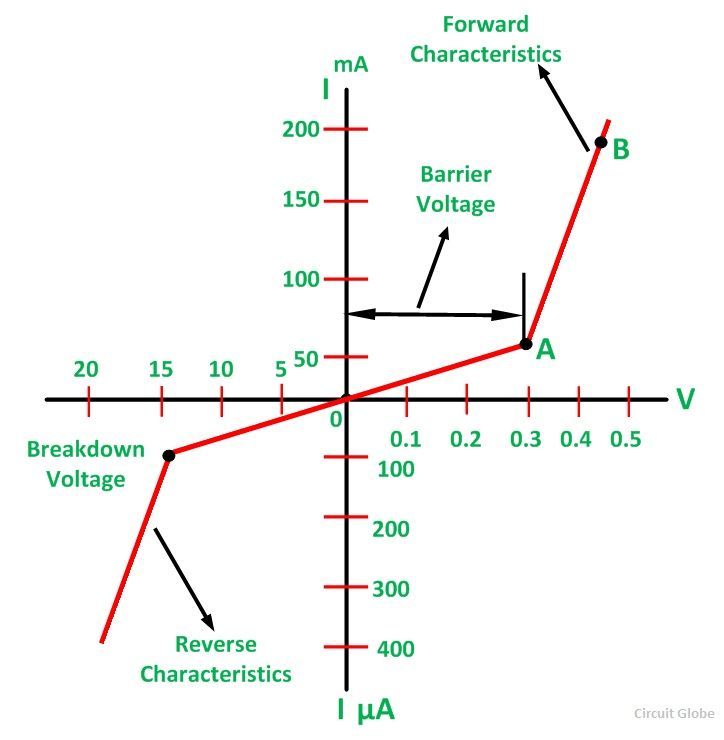
The volt-ampere or V- I characteristics of a semiconductor diode is a curve between the voltage across the junction and the circuit current.
The circuit arrangement is shown below.
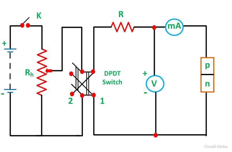
The resistor R is connected in series with the PN junction which limits the diode forward current from exceeding the prescribed limit value. The characteristics are studied under three heads i.e. zero external voltage, forward biasing, and reverse biasing. They are described below in detail.
Zero External Voltage
When no external voltage is applied that is the circuit is open at key K, no current flows through the circuit. It is indicated by point 0 on the graph shown below:
Forward Biasing
When key K is closed and the double throw switch is thrown to position 1 as shown in the above circuit diagram A. The PN junction is forward biased as a p-type semiconductor is connected to the positive terminal and n-type to the negative terminal of the supply. Now, when the supply voltage is increased by changing the variable resistor Rh. The circuit current increases very slowly and the curve is non-linear shown in the above characteristic figure B as OA.
The slow rise in the current in this region is because the externally applied voltage is used to overcome the potential barrier of 0.3 V for Ge and 0.7 for Si of the PN junction. However, once the potential barrier is eliminated and the external supply voltage is increased further. The PN junction behaves like an ordinary conductor and the circuit current rises very sharply represented by the region AB.
At this instant, the current is limited by the series resistance R and a small value of the junction forward resistance Rf. The curve is almost linear. If the current rises more than the rated value of the diode, the diode may be damaged.
Knee Voltage
The forward voltage (0.3 V for Ge and 0.7 V for Si diodes) at which the current through the diode or p n junction starts rising abruptly is known as Knee Voltage.
Reverse Biasing
When the double pole double throw (DPDT) switch is thrown to position 2 as shown in figure A. The p n junction is reverse biased as a p-type semiconductor is connected to the negative terminal and n-type to the positive terminal of the supply. Under this condition, the potential barrier at the junction is increased. Therefore, the junction resistance Rr becomes very high and practically no current flows through the circuit.
However, in actual practice a very small current of the order of microampere flow in the circuit. This current is known as Reverse Current and is due to minority carriers available at room temperature.
The reverse current increases slightly with the increase in reverse bias supply voltage. If the reverse voltage is increased continuously, a stage reaches when the kinetic energy of electrons (minority carriers) becomes so high that they knock out electrons from the semiconductor bonds. At point C, the breakdown of the junction occurs and the resistance of the barrier region Rr falls suddenly.
Consequently, the reverse current rises tremendously to a large value. This may destroy the junction permanently. The reverse voltage at which the p n junction breaks is known as Breakdown Voltage.
The following points are concluded from all the above discussion.
- At zero external voltage, no current flows through the circuit or diode.
- At forward bias, the current increases slightly till the barrier potential is wiped off.
- After Knee voltage, the forward current rises drastically.
- The forward current is limited by the series resistance R and a small value of junction resistance Rf.
- The diode gets destroyed as the forward current increases beyond the rated value of the diode.
- The reverse current increases slightly with the increase in voltage because of the minority carriers. The maximum value of reverse current for Si diode is as low as 1 microampere. For Ge, it is about 100 microampere.
- The reverse voltage at which junction breaks is known as the breakdown voltage.
- At reverse voltage, when the junction breaks the diode may be destroyed.
This is all about the semiconductor diode.
Nice article, i will share it forward
Very good way of understanding electronics