Definition: The transistor in which one p-type material is placed between two n-type materials is known as NPN transistor. The NPN transistor amplifies the weak signal enter into the base and produces strong amplify signals at the collector end. In NPN transistor, the direction of movement of an electron is from the emitter to collector region due to which the current constitutes in the transistor. Such type of transistor is mostly used in the circuit because their majority charge carriers are electrons which have high mobility as compared to holes.
Construction of NPN Transistor
The NPN transistor has two diodes connected back to back. The diode on the left side is called an emitter-base diode, and the diodes on the left side are called collector-base diode. These names are given as per the name of the terminals.
 The NPN transistor has three terminals, namely emitter, collector and base. The middle section of the NPN transistor is lightly doped, and it is the most important factor of the working of the transistor. The emitter is moderately doped, and the collector is heavily doped.
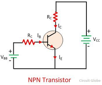
Circuit Diagram of NPN Transistor
The circuit diagram of the NPN transistor is shown in the figure below. The collector and the base circuit is connected in reverse biased while the emitter and base circuit is connected in forward biased. The collector is always connected to the positive supply, and the base is in negative supply for controlling the ON/OFF states of the transistor.
Working of NPN Transistor
The circuit diagram of the NPN transistor is shown in the figure below. The forward biased is applied across the emitter-base junction, and the reversed biased is applied across the collector-base junction. The forward biased voltage VEB is small as compared to the reverse bias voltage VCB.
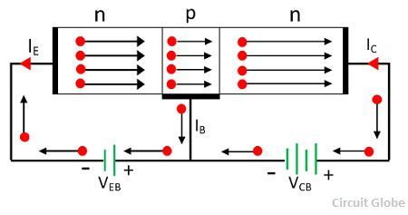
The emitter of the NPN transistor is heavily doped. When the forward bias is applied across the emitter, the majority charge carriers move towards the base. This causes the emitter current IE. The electrons enter into the P-type material and combine with the holes.
The base of the NPN transistor is lightly doped. Due to which only a few electrons are combined and remaining constitutes the base current IB. This base current enters into the collector region. The reversed bias potential of the collector region applies the high attractive force on the electrons reaching collector junction. Thus attract or collect the electrons at the collector.
The whole of the emitter current is entered into the base. Thus, we can say that the emitter current is the sum of the collector and the base current.
it is very helpful
It’s very good and it’s also useful and easy to understand
very good write up hopefully help me pass my course work
This is a very helpful when you have less time for revision 🙏
WELL EXPLAINED, CONTINUE WITH THE SAME. THANK U
Finally I found this 🙌
Well explained
Thanks
Include it’s operation in saturation mode… Otherwise nice explanation
Simple and easy to understand 😁