One of the major difference between the NPN and PNP transistor is that in the NPN transistor the current flow between collector to emitter when the positive supply is given to the base, whereas in PNP transistor the charge carrier flows from the emitter to collector when negative supply is given to the base. The NPN and PNP transistor are differentiated below in the comparison chart by considering the various other factors.
The NPN and PNP both are the bipolar junction transistor. It is the current controlling devices and mainly used for switching and amplifying the signal. Mostly, the NPN transistor is used in the circuit because in NPN transistor the conduction current is mainly by electrons while in the PNP transistor the conduction current is because of the holes. As the electrons are more mobile the NPN has high conduction.
The letter PNP and NPN show the voltage requires by the emitter, collector and base of the junction transistor. The NPN and PNP transistor, both are made up of different material due to which the current develops in them also differs. Sometimes when the voltage applied across the emitter the electrons cross the base junction and reach the collector region. This happens because the base of the NPN and PNP transistor is very thin and lightly doped.
Content: NPN Vs PNP Transistor
Comparison Chart
| Basis For Comparison | NPN Transistor | PNP Transistor |
|---|---|---|
| Definition | Transistor in which two n-type layer are separated by one P-type layer | Two blocks of p- types semiconductors are separated by one thin block of n-type semiconductor. |
| Symbol | 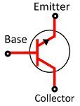 | 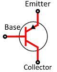 |
| Full Form | Negative Positive and Negative | Positive Negative and Positive |
| Direction of Current | Collector to Emitter | Emitter to Collector |
| Turn-on | When electrons enters into the base. | When holes enter into the base. |
| Inside Current | Develop because of varying position of electrons. | Originate because of varying position of holes. |
| Outside Current | Current develop because of the flow of holes. | Current develop because of the flow of electrons. |
| Majority Charge Carrier | Electron | Hole |
| Switching Time | Faster | Slower |
| Minority Charge Carrier | Hole | Electron |
| Positive Voltage | Collector Terminal | Emitter Terminal |
| Forward Biased | Emitter Base Junction | Emitter Base Junction |
| Reverse Biased | Collector Base Junction | Collector Base Junction |
| Small current | Flows from emitter-to-base | Base to emitter |
| Ground Signal | Low | High |
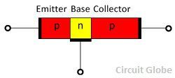
Definition of PNP Transistor
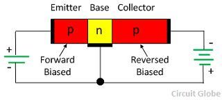
The PNP transistor has two blocks of p-type material and one block of n-type material. It has three terminals emitter, base and collector. The emitter and collector of PNP transistor are made up of p-type material and their base is made up of n-type material.
 The emitter-base junction of PNP is connected in forward biased while the collector-base junction is connected in reverse bias. The emitter-base junction pushes the majority charge carrier toward the base, thus established the emitter current. The hole in the p-type material combines with the n-type material hence constitute the base current. The remaining hole reaches across the negatively biased collector-base region and collected by the collector due to which collector current develops. Thus, complete emitter current flows through the collector circuit.
Emitter Current = Collector Current + Base Current
 Definition of NPN Transistor
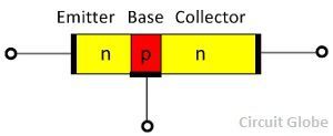
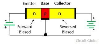
The NPN transistor consists two n-type semiconductor material which is separated by a thin layer of p-type material. The collector is the thickest region and the base is the thinnest region of the NPN transistor. The emitter-base region of the transistor is in forward biasing and the collector base region is connected in reverse bias. The voltage of the reverse bias is considerably smaller as compared to the reversed biased.
 The emitter-base junction is in forward biasing due to which a large number of electrons is reached to the base. This develops the emitter current. The electron in the base region combined with the holes. But the base is very thin and lightly doped, thus only small holes combined with the electrons and constitute the base current. The remaining electrons reach across the collector base region and develop the collector current. The entire emitter current flows through the collector circuit.
Emitter Current = Collector Current + Base Current
Key Differences Between NPN and PNP Transistor
- The NPN transistor has two blocks of n-type semiconductor materials and one block of p types semiconductor materials whereas the PNP transistor has one thin layer of p-type material and two thick layers of N-type material.
- The symbol of the NPN and the PNP transistor are almost same the only difference between them is the direction of the arrow which is based on the emitter. In NPN transistor the head of the arrow move outward to the base and in PNP the arrow moves inward.
- In NPN transistor, the current flow from collector to emitter because positive supply is given to the base, whereas, in PNP transistor the current flows from the emitter to the collector.
- The NPN transistor turn-on when the electron enters into the base while the PNP transistor is turned on when holes enter into the base.
- The inside current in NPN transistor constitutes because of the varying position of the electrons whereas in PNP transistor the inside current is because of the varying position of the holes.
- In NPN transistor the output current exists because flows of the holes and in PNP it is constituted because of the flows of the electrons.
- In NPN transistor, the majority charge carrier is electron whereas in PNP transistor the majority hole is the majority charge carrier.
- The minority charge carrier of the NPN transistor is the hole and in PNP transistor it is electrons.
- The switching time of NPN transistor is more as compared to PNP transistor because the majority charge carrier of NPN transistor is an electron.
- The emitter-base junction of both the NPN and PNP transistor is connected in forward biased.
- Note: The forward base junction means the p terminal of the diode is connected to the positive terminal of the supply and the n-type material is connected to the negative terminal of the supply
- The collector base junction of the NPN and PNP transistor is connected in reversed biased.
- Note: The reversed bias means the negative region is connected to the positive terminal of the supply and the p-region is connected to the positive terminal of the supply.
- The NPN transistor turns on when the small current flows from emitter to base, whereas for turning on the PNP transistor the small current flows from base to emitter.
- The ground signal of the PNP transistor is kept low, whereas, in PNP transistor the ground signal is high.
The key to the transistor action is lightly doped base between the heavily doped collector and emitter.
Nice Content.
Useful.. Thankyou
Very knowledgeable article & Useful Thank you.
Very knowledgeable and helpful…
wow ..nicely explained..!
Very Helpful