Definition: The fabrication of the transistor is the process of creating the transistor that is used in electrical and electronics circuit. It is a photo-lithographic or chemical process of creating the transistor on the wafer of semiconductor material.
Mostly silicon is used for the fabrication. But compound semiconductor is also used for the manufacturing of the transistor. The entire process of transistor fabrication requires 6 – 8 days. The avalanche junction and diffused junction are the technique used for the fabrication of the transistor. These techniques are explained below in details.
Alloy-Junction Technique
The alloy-junction technique is very less expensive and provides less current gain. It is the earliest technique of fabrication of transistors. The transistor which is built by using an alloy junction technique is capable of handling the maximum rating of current and power. The fabrication technique of making germanium alloy junction PNP transistor is shown in the figure below.
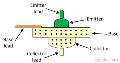
The very thin layer of germanium crystal wafer is taken. The wafer is lightly doped and taken as a base of the transistor. The indium dots (p-type impurity) are taken on both the side of the wafer and heated. The heat should be maintained in such a manner that the temperature should be raised above the melting point of indium but below the melting point of germanium. The liquid solution of germanium is obtained in indium.
 The whole structure is cooled down steadily. After cooling, the region of p-type germanium is produced, and the alloy of indium and germanium is deposited on the layer. The lead of the emitter and collector deposits on the two sides of the wafer as shown in the figure below. Thus, PNP transistor is fabricated.
Diffused Junction Technique
In this technique, the alternate p-type and n-type impurities are gaseously diffuse into the wafer of semiconductor material at high temperature for forming the emitter and collector junction. The diffusion type silicon transistor is shown in the figure below.
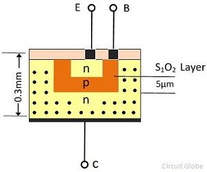
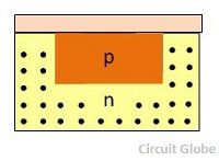
The n-type silicon wafer is used for making the collector terminal. On the surface of the silicon wafer, Silicon oxide (SiO2) is grown. The silicon-di-oxide is an insulating material which does not allow the impurities to enter through it.
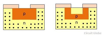
 For making the wafer, the acceptor type impurities are diffused into the wafer. For this, the SiO2 layer is removed from the area from where the base is to be spread. The born impurities are exposed in the form of the vapour, and hence the impurity is added to the depth of the material as shown in the figure below. Thus, the base region of P-type material develops.
 The another layer of SiO2 material is grown over the entire wafer of the transistor.
The part of SiO2 is grown over shown in the figure below. The layer of SiO2 is again engraved over the wafer of donor type impurities (e.g. Phosphorous). Thus, the n-type emitter region is built.
The metal contacts are engraved on the surface shown above in the figure. The wafer exhibit on the suitable collector contacts and then cut into the required size.
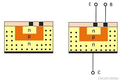 The leads are then connected to the base emitter and collector shown above.