Definition: The transistor in which one n-type material is doped with two p-type materials such type of transistor is known as PNP transistor. It is a current controlled device. The small amount of base current controlled both the emitter and collector current. The PNP transistor has two crystal diodes connected back to back. The left side of the diode in known as the emitter-base diode and the right side of the diode is known as the collector-base diode.
The hole is the majority carriers of the PNP transistors which constitute the current in it. The current inside the transistor is constituted because of the changing position of holes and in the leads of the transistor it is because of the flow of the electrons. The PNP transistor turns on when a small current flows through the base. The direction of current in PNP transistor is from the emitter to collector.
The letter of the PNP transistor indicates the voltage requires by the emitter, collector and the base of the transistor. The base of the PNP transistor has always been negative with respect to the emitter and collector. In PNP transistor, the electrons are taken from the base terminal. The current which enters into the base is amplified into the collector ends.
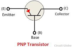
Symbol of PNP Transistor
The symbol of PNP transistor is shown in the figure below. The inward arrow shows that the direction of current in PNP transistor is from the emitter to collector.
Construction of PNP Transistor
The construction of PNP transistor is shown in the figure below. The emitter-base junction is connected in forward biased, and the collector-base junction is connected in reverse biased. The emitter which is connected in the forward biased attracts the electrons towards the battery and hence constitutes the current to flow from emitter to collector.
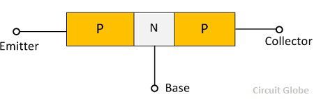
The base of the transistor is always kept positive with respect to the collector so that the hole from the collector junction cannot enter into the base. And the base-emitter is kept in forward due to which the holes from the emitter region enter into the base and then into the collector region by crossing the depletion region.
Working of PNP Transistor
The emitter-base junction is connected in forward biased due to which the emitter pushes the holes in the base region. These holes constitute the emitter current. When these electrons move into the N-type semiconductor material or base, they combined with the electrons. The base of the transistor is thin and very lightly doped. Hence only a few holes combined with the electrons and the remaining are moved towards the collector space charge layer. Hence develops the base current.
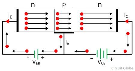
The collector base region is connected in reverse biased. The holes which collect around the depletion region when coming under the impact of negative polarity collected or attracted by the collector. This develops the collector current. The complete emitter current flows through the collector current IC.
Nice explained
It’s helpful for me. Thank you very much for clearly explaining this topic …now I’m confident to write this in my examination….thanks
Thank you so much ……it has been of great help…..
It’s helpful for me.thank you very much for clearly explaining this topic ..thank you so much
Well explained
WELL EXPLAINED
Best
Really super well explained
Very helpful …..
Can be used as a project…
Well explained…
Thanks for the help…
Easy to understand..