Definition: The diode in which the intrinsic layer of high resistivity is sandwiched between the P and N-region of semiconductor material such type of diode is known as the PIN diode. The high resistive layer of the intrinsic region provides the large electric field between the P and N-region. The electric field induces because of the movement of the holes and the electrons. The direction of the electric field is from n-region to p-region.
The high electric field generates the large electron holes pairs due to which the diode process even for the small signals. The PIN diode is a type of photodetector used for converting the light energy into the electrical energy.
The intrinsic layer between the P and N-type regions increases the distance between them. The width of the region is inversely proportional to their capacitance. If the separation between the P and N region increases their capacitance decreases. This characteristic of diode increases their response time and makes the diode suitable for works like a microwaves applications.
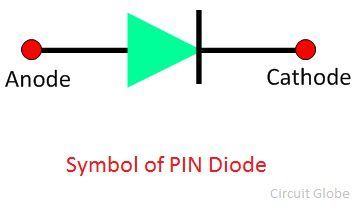
Symbol of PIN Diode
The symbolic representation of the PIN diode is shown in the figure below. The anode and cathode are the two terminal of the PIN diode. The anode is the positive terminal and cathode represent their negative terminals.
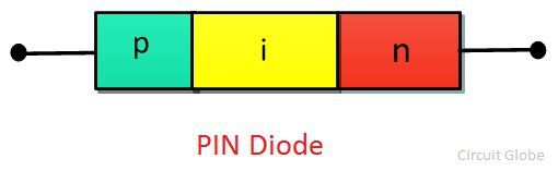
PIN Diode Structure
The diode consists the P-region and N-region which is separated by the intrinsic semiconductor material. In P-region the hole is the majority charge carrier while in n-region the electron is the majority charge carrier. The intrinsic region has no free charge carrier. It acts as an insulator between n and the p-type region. The i-region has the high resistance which obstructs the flow of electrons to pass through it.
Working of PIN Diode
The working of the PIN diode is similar to the ordinary diode. When the diode is unbiased, their charge carrier will diffuse. The word diffusion means the charge carriers of the depletion region try to move to their region. The process of diffusion occurs continue until the charges become equilibrium in the depletion region.
Let the N and I-layer make the depletion region. The diffusion of the hole and electron across the region generates the depletion layer across the NI-region. The thin depletion layer induces across n-region, and thick depletion region of opposite polarity induces across the I-region.
Forward Biased PIN Diode
When the diode is kept forward biased, the charges are continuously injected into the I-region from the P and N-region. This reduces the forward resistance of the diode, and it behaves like a variable resistance.
The charge carrier which enters from P and N-region into the i-region are not immediately combined into the intrinsic region. The finite quantity of charge stored in the intrinsic region decreases their resistivity.
Consider the Q be the quantity of charge stored in the depletion region. The τ be the time used for the recombination of the charges. The quantity of the charges stored in the intrinsic region depends on their recombination time. The forward current starts flowing into the I region.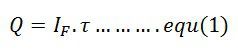
Where, IF – forward current
τ- recombination time
The resistance (Rs) of the current under forwarding biased is inversely proportional to the charge Q stored in the intrinsic region.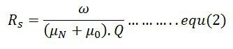
Where, w – width region
μ – electron mobility
μ0 – hole mobility
From equation (1) and (2), we get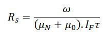
The above equation shows that the resistance of the intrinsic region depends on the width of the region.
Reversed Biased PIN Diode
When the reverse voltage is applied across the diode, the width of the depletion region increases. The thickness of the region increases until the entire mobile charge carrier of the I-region swept away from it. The reverse voltage requires for removing the complete charge carrier from the I-region is known as the swept voltage.
In reverse bias, the diode behaves like a capacitor. The P and N region acts as the positive and negative plates of the capacitor, and the intrinsic region is the insulator between the plates.
Where, A – junction diode
w – intrinsic region thickness
The lowest frequency at which the effect starts to begins is expressed as
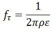
Where, ε – silicon dielectric constant
Applications of PIN Diode
- High Voltage Rectifier – It is used as a high voltage rectifier. The diode has a large intrinsic region between the N and P-region which can tolerate the high reverse voltage.
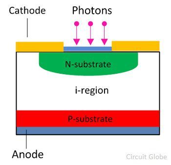
- Photo-detector – The PIN diode is used for converting the light energy into the electrical energy. The diode has large depletion region which improves their performance by increasing the volume of light conversion.
The PIN diode is most suitable for low voltage applications.