Definition: The phototransistor is a three-layer semiconductor device which has a light-sensitive base region. The base senses the light and converts it into the current which flows between the collector and the emitter region.
The construction of phototransistor is similar to the ordinary transistor, except the base terminal. In phototransistor, the base terminal is not provided, and instead of the base current, the light energy is taken as the input.
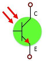
Symbol of Phototransistor
The symbol of the phototransistor is similar to that of the ordinary transistor. The only difference is that of the two arrows which show the light incident on the base of the phototransistor.
 Principle of Phototransistor
Consider the conventional transistor is having open terminal base circuited. The collector base leakage current acts as a base current ICBO.
IC = βIB + (1+B) ICBO
As the base current IB = 0, It acts as an open circuited. And the collector current becomes.
IC = (1+B) ICBO
The above equations shown that the collector current is directly proportional to the current base leakage current, i.e., the IC increases with the increases of the collector base region.
Phototransistor Operation
The phototransistor is made up of semiconductor material. When the light was striking on the material, the free electrons/holes of the semiconductor material causes the current which flows in the base region. The base of the phototransistor would only be used for biasing the transistor. In case of NPN transistor, the collector is made positive concerning emitter, and in PNP, the collector is kept negative.
The light enters into the base region of phototransistor generates the electron-hole pairs. The generation of electron-hole pairs mainly occurs into the reverse biasing. The movement of electrons under the influence of electric field causes the current in the base region. The base current injected the electrons in the emitter region. The major drawback of the phototransistor is that they have low-frequency response.
Phototransistor Construction
The construction of the phototransistor is quite similar to the ordinary transistor. Earlier, the germanium and silicon are used for fabricating the phototransistor. The small hole is made on the surface of the collector-base junction for placing the lens. The lens focuses the light on the surface.
 Nowadays the transistor is made of a highly light effective material (like gallium and arsenides). The emitter-base junction is kept at forward biased, and the collector-base junction is at the reverse biased.
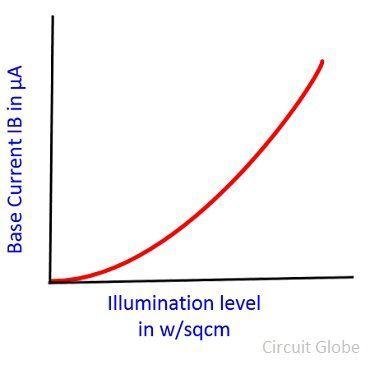
When no light falls on the surface of the transistor, the small reverse saturation current induces on the transistor. The reverse saturation current induces because of the few minority charge carriers. The light energy falls on the collector-base junction and generates the more majority charge carrier which adds the current to the reverse saturation current. The graph below shows the magnitude of current increases along with the intensity of light.
 The phototransistor is widely used in electronics devices likes smoke detectors, infrared receiver, CD players, lasers etc. for sensing light.
Photodiode Vs Phototransistor
The photodiode and phototransistor both convert the light energy into the electrical energy. But the phototransistor is mostly preferred over the photodiode because of their following advantages.
- The current gain in the phototransistor is more than the phototransistor even if the same amount of light strike on it.
- The sensitivity of the phototransistor is higher than the photodiode.
- The photodiode can be converted into the phototransistor by removing their emitter terminals.
The response time of the photodiode is much higher than the phototransistor. The output current of the photodiode is in microamperes, and it can switch on or off in nanoseconds. While the response time of the phototransistor is in microseconds and it provides current in milliamperes.
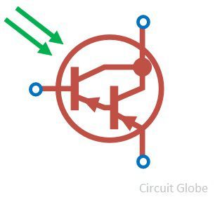
Photodarlington
In photodarlington, the two transistor connected back to back through the base shown in the figure below. In this arrangement, the phototransistor induces much higher power, i.e., their sensitivity rises.
 The photodarlington transistor has large switching time. The devices are used in the integrated amplifier and in the photosensitive SCRs amplifier etc.