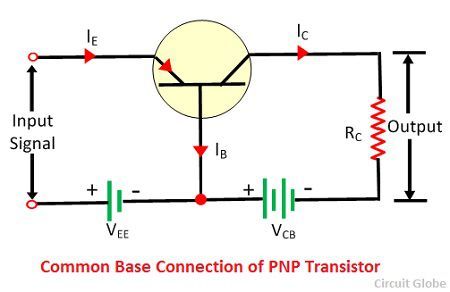
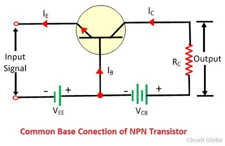
Definition: The configuration in which the base of the transistor is common between emitter and collector circuit is called a common base configuration. The common base circuit arrangement for NPN and PNP transistor is shown in the figure below. In common base-emitter connection, the input is connected between emitter and base while the output is taken across collector and base.
Current Amplification factor (α)
The ratio of output current to input current is known as a current amplification factor. In the common base configuration, the collector current IC is the output current, and the emitter current IE is the input current. Thus, the ratio of change in emitter current to the collector at constant collector-base voltage is known as a current amplification factor of a transistor in common base configuration. It is represented by α (alpha).

Where ΔIC is the change in the collector and ΔIE is changed in emitter current at constant VCB. Now,
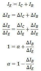
The value of current amplification factor is less than unity. The value of the amplification factor (α) reaches to unity when the base current reduces to zero. The base current becomes zero only when it is thin and lightly doped. The practical value of the amplification factor varies from 0.95 to 0.99 in the commercial transistor.
Collector Current
The base current is because of the recombination of the electrons and holes in the base region. The whole emitter current will not flow through the current. The collector current increase slightly because of the leakage current flows due to the minority charge carrier. The total collector current consists;
- The large percentage of emitter current that reaches the collector terminal, i.e., αIE.
- The leakage current Ileakage. The minority charge carrier is because of the flow of minority charge carrier across the collector-base junction as the junction is heavily reversed. Its value is much smaller than αIE.
Total collector current,
![]()
The above expression shows that if IE = 0 (when the emitter circuit is open) then still a small current flow in the collector circuit called leakage current. This leakage current is represented by as ICBO, i.e., collector-base current with emitter circuit is open.
![]()
The leakage current is also abbreviated as ICO i.e., the collector current with emitter circuit open.
Characteristics of Common Base (CB) Configuration
The characteristic diagram of determining the common base characteristic is shown in the figure below.
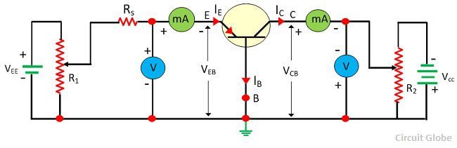
The emitter to base voltage VEB can be varied by adjusting the potentiometer R1. A series resistor RS is inserted in the emitter circuit to limit the emitter current IE. The value of the emitter change to a large value even the value of a potentiometer slightly change. The value of collector voltage changes slightly by changing the value of the potentiometer R2. The input and output characteristic curve of the potentiometer explains below in details.
Input Characteristic
The curve plotted between emitter current IE and the emitter-base voltage VEB at constant collector base voltage VCB is called input characteristic curve. The input characteristic curve is shown in the figure below.
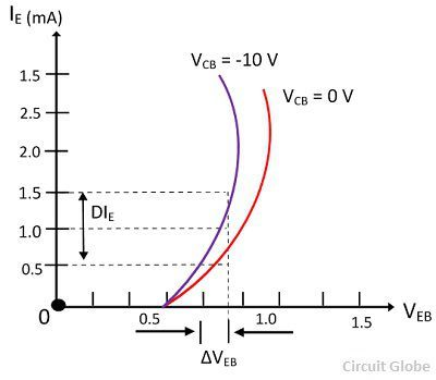
The following points are taken into consideration from the characteristic curve.
- For a specific value of VCB, the curve is a diode characteristic in the forward region. The PN emitter junction is forward biased.
- When the value of the voltage base current increases the value of emitter current increases slightly. The junction behaves like a better diode. The emitter and collector current is independent of the collector base voltage VCB.
- The emitter current IE increases with the small increase in emitter-base voltage VEB. It shows that input resistance is small.
Input Resistance
The ratio of change in emitter-base voltage to the resulting change in emitter current at constant collector base voltage VCB is known as input resistance. The input resistance is expressed by the formula
The value of collector base voltage VCB increases with the increases in the collector-base current. The value of input resistance is very low, and their value may vary from a few ohms to 10 ohms.
Output Characteristic Curve
In common base configuration, the curve plotted between the collector current and collector base voltage VCB at constant emitter current IE is called output characteristic. The CB configuration of PNP transistor is shown in the figure below. The following points from the characteristic curve are taken into consideration.
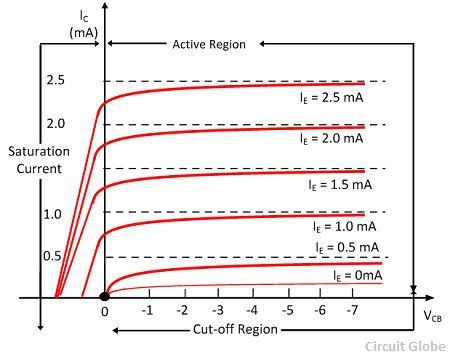
- The active region of the collector-base junction is reverse biased, the collector current IC is almost equal to the emitter current IE. The transistor is always operated in this region.
- The curve of the active regions is almost flat. The large charges in VCB produce only a tiny change in IC The circuit has very high output resistance ro.
- When VCB is positive, the collector-base junction is forward bias and the collector current decrease suddenly. This is the saturation state in which the collector current does not depend on the emitter current.
- When the emitter current is zero, the collector current is not zero. The current which flows through the circuit is the reverse leakage current, i.e., ICBO. The current is temperature depends and its value range from 0.1 to 1.0 μA for silicon transistor and 2 to 5 μA for germanium transistor.
Output Resistance
The ratio of change in collector-base voltage to the change in collector current at constant emitter current IE is known as output resistance.
The output characteristic of the change in collector current is very little with the change in VCB. With the change in collector-base voltage. The output resistance is very high of the order of several kilometres.
Very nice 👌
Which is the suitable type of transistor and number of transistor ?