Definition: The potential barrier in the PN-junction diode is the barrier in which the charge requires additional force for crossing the region. In other words, the barrier in which the charge carrier stopped by the obstructive force is known as the potential barrier.
How It gets established?
When the P and N-type semiconductor material are placed together, the gradient of very large density charge carriers is created on both the P and N side region. The free electrons from N-side cross the region and start combining with the holes, leaving behind the immobile positive donor ions. Similarly, the holes of the P-region combine with the electrons of the N-region and leaving behind the negative acceptor ions.
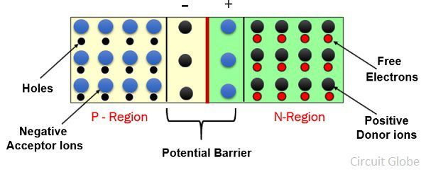
The process is continued until the P and N-region have enough charge carrier for opposing the electrons and holes respectively. The immobile ions (negative acceptor ions and positive donor ions) are concentrated between the N and P-region and create the electric field which acts as a barrier between the flows of charges.The region is created because of the depleted ions, and hence it is called the depletion region.
The depletion region acts as a barrier and opposes the flow of charge carrier. The value of barrier potential lies between 0.3 – 0.7V depends on the type of material used.