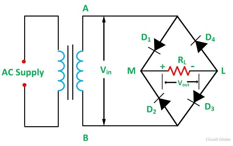
In Full Wave Bridge Rectifier, an ordinary transformer is used in place of a center-tapped transformer. The circuit forms a bridge connecting the four diodes D1, D2, D3, and D4. The circuit diagram of the Full Wave Bridge Rectifier is shown below.
Contents:
- Operation of Full Wave Bridge Rectifier
- Peak Inverse Voltage of Full Wave Bridge Rectifier
- Advantages of Full Wave Bridge Rectifier
- Disadvantages of Full Wave Bridge Rectifier
The AC supply which is to be rectified is applied diagonally to the opposite ends of the bridge. Whereas, the load resistor RL is connected across the remaining two diagonals of the opposite ends of the bridge.
Operation of Full Wave Bridge Rectifier
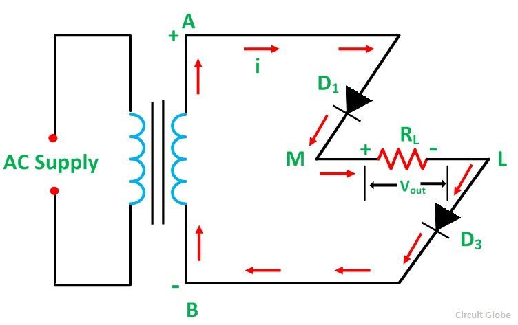
When an AC supply is switched ON, the alternating voltage Vin appears across the terminals AB of the secondary winding of the transformer which needs rectification. During the positive half cycle of the secondary voltage, end A becomes positive, and end B becomes negative as shown in the figure below.
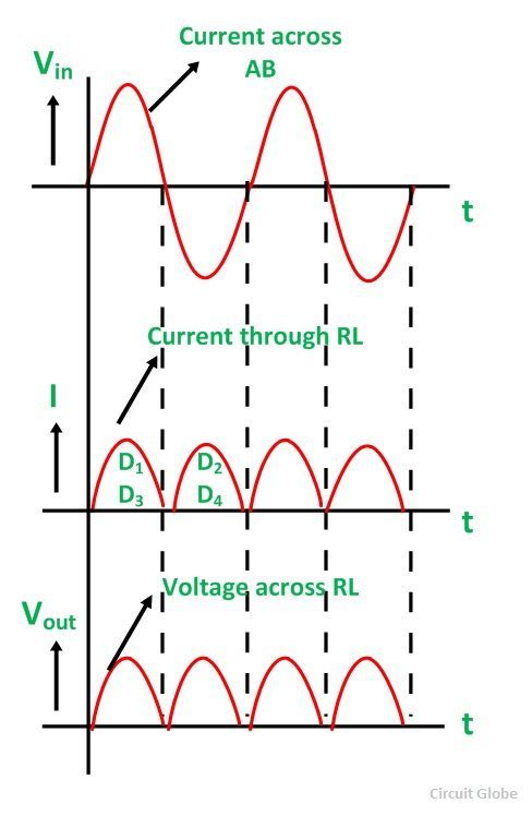
The diodes D1 and D3 are forward biased and the diodes D2 and D4 are reversed biased. Therefore, diode D1 and D3 conduct, and diode D2 and D4 do not conduct. The current (i) flows through diode D1, load resistor RL (from M to L), diode D3, and the transformer secondary. The waveform of the full-wave bridge rectifier is shown below.
During the negative half-cycle, end A becomes negative and end B positive as shown in the figure below:
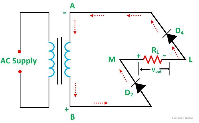
From the above diagram, it is seen that the diode D2 and D4 are under forward bias and the diodes D1 and D3 are reverse bias. Therefore, diode D2 and D4 conduct while diodes D1 and D3 do not conduct. Thus, current (i) flows through the diode D2, load resistor RL (from M to L), diode D4, and the transformer secondary.
The current flows through the load resistor RL in the same direction (M to L) during both the half cycles. Hence, a DC output voltage Vout is obtained across the load resistor.
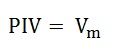
Peak Inverse Voltage of Full Wave Bridge Rectifier
When the secondary voltage attains its maximum positive value and the terminal A is positive, and B is negative as shown in the circuit diagram below.
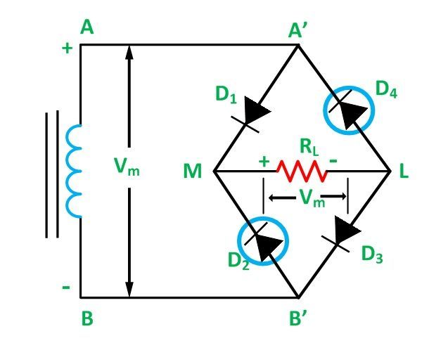
At this instant diode, D1 and D3 are forward biased and conducts current. Therefore, terminal M attains the same voltage as that A’ or A, whereas the terminal L attains the same voltage as that of B’ or B. Hence the diode D2 and D4 are reversed biased and the peak inverse voltage across both of them is Vm.
Therefore,
Advantages of Full Wave Bridge Rectifier
- The center tap transformer is eliminated.
- The output is double that of the center-tapped full-wave rectifier for the same secondary voltage.
- The peak inverse voltage across each diode is one-half of the center tap circuit of the diode.
Disadvantages of Full Wave Bridge Rectifier
- It needs four diodes.
- The circuit is not suitable when a small voltage is required to be rectified. It is because, in this case, the two diodes are connected in series and offer double voltage drop due to their internal resistance.
Also See: Half Wave and Full Wave Rectifier