An Adder is a device that can add two binary digits. It is a type of digital circuit that performs the operation of additions of two number. It is mainly designed for the addition of binary number, but they can be used in various other applications like binary code decimal, address decoding, table index calculation, etc.
There are two types of Adder. One is Half Adder, and another one is known as Full Adder. The detailed explanation of the two types of adder is given below.
Half Adder
There are two inputs and two outputs in a Half Adder. Inputs are named as A and B, and the outputs are named as Sum (S) and Carry (C). The Sum is X-OR of the input A and B. Carry is AND of the input A and B. With the help of half adder, one can design a circuit that is capable of performing simple addition with the help of logic gates.
Let us first take a look at the addition of single bits.
0 + 0 = 0
0 + 1 = 1
1 + 0 = 1
1 + 1 = 10
These are the least possible single bit combinations. But the result for 1 + 1 =10. This problem can be solved with the help of an EX-OR gate. The sum results can be re-written as a 2-bit output.
Thus the above combination can be written as:
0 + 0 = 00
0 + 1 = 01
1 + 0 = 01
1 + 1 = 10
Here the output “1” of “10” becomes the carry-out. SUM is the normal output and the CARRY is the carry-out.
The truth table of the half adder is shown below:
| Inputs | Outputs | ||
|---|---|---|---|
| A | B | Sum | Carry |
| 0 | 0 | 0 | 0 |
| 0 | 1 | 1 | 0 |
| 1 | 0 | 1 | 0 |
| 1 | 1 | 0 | 1 |
The Half Adder Circuit is shown below:
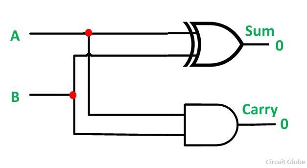 The main disadvantage of this circuit is that it can only add two inputs and if there is any carry, it is neglected. Thus, the process is incomplete.
To overcome this difficulty Full Adder is designed. While performing complex addition, there may be cases when you have to add two 8 bit bytes together. This can be done with the help of Full Adder.
Full Adder
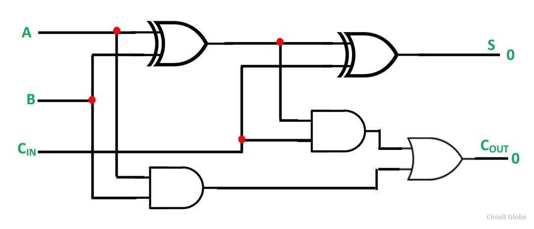
The full adder is a little more difficult to implement than a half adder. The main difference between a half adder and a full adder is that the full-adder has three inputs and two outputs. The two inputs are A and B, and the third input is a carry input CIN. The output carry is designated as COUT, and the normal output is designated as S.
The truth table of the Full Adder Circuit is shown below.
| Inputs | Outputs | |||
|---|---|---|---|---|
| A | B | CIN | COUT | S |
| 0 | 0 | 0 | 0 | 0 |
| 0 | 0 | 1 | 0 | 1 |
| 0 | 1 | 0 | 0 | 1 |
| 0 | 1 | 1 | 1 | 0 |
| 1 | 0 | 0 | 0 | 1 |
| 1 | 0 | 1 | 1 | 0 |
| 1 | 1 | 0 | 1 | 0 |
| 1 | 1 | 1 | 1 | 1 |
The output S is an EX-OR between the input A and the half-adder SUM output B. The COUT will be true only if any of the two inputs out of the three are HIGH or at logic 1.
Thus, a full adder circuit can be implemented with the help of two half adder circuits. The first half adder circuit will be used to add A and B to produce a partial sum. The second half adder logic can be used to add CIN to the sum produced by the first half adder circuit. Finally, the output S is obtained.
If any of the half adder logic produces a carry, there will be an output carry. Thus, COUT will be an OR function of the half adder CARRY outputs.
The Full adder circuit diagram is shown below:
 The schematic representation of a single bit Full Adder is shown below:
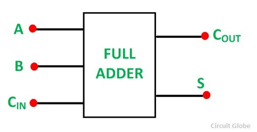 With the help of this type of symbol, one can add two bits together, taking a carry from the next lower order of magnitude and sending a carry to the next higher order of magnitude.
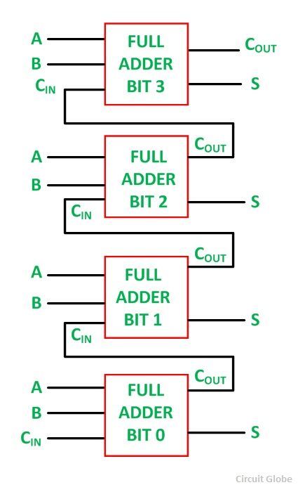
In a computer, for a multi-bit operation, each bit must be represented by a full adder and must be added simultaneously. Thus, to add two 8 bit numbers, 8 full address is needed that can be formed by cascading two of the 4-bit blocks.
The addition of the four-bit number is shown below:
 Full Adder is used for a complex addition like for adding two 8 – bit bytes together.
Your Website is very useful for us.
Thanks you. It’s great!
Thanks sir.
Really a helpful topic sir….thanks alot…
It’s really helped us. Thanks for your great works.
This is very helpful.
Keep developing your site bro
It’s very helpful
Thnxxxxx
this is very usefull for any user
thnxxxxxxxxxxxxxxxxxx!!!!!!
ya its very helpful
Useful article
Thank U very much
Thank you ☺️