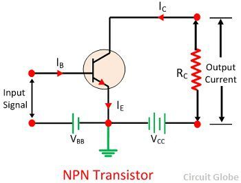
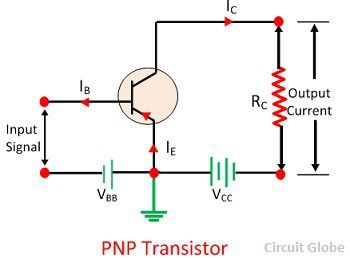
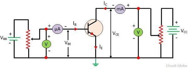
Definition: The configuration in which the emitter is connected between the collector and base is known as a common emitter configuration. The input circuit is connected between emitter and base, and the output circuit is taken from the collector and emitter. Thus, the emitter is common to both the input and the output circuit, and hence the name is the common emitter configuration. The common emitter arrangement for NPN and PNP transistor is shown in the figure below.
Base Current Amplification Factor (β)
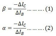
The base current amplification factor is defined as the ratio of the output and input current in a common emitter configuration. In common emitter amplification, the output current is the collector current IC, and the input current is the base current IB.
In other words, the ratio of change in collector current with respect to base current is known as the base amplification factor. It is represented by β (beta).

Relation Between Current Amplification Factor (α) & Base Amplification Factor (β)
The relation between Β and α can be derived as
We Known,
Now,
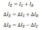
Substituting the value of ΔIE in equation (1), we get,
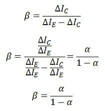 The above equation shows that the when the α reaches to unity, then the β reaches to infinity. In other words, the current gain in a common emitter configuration is very high, and because of this reason, the common emitter arrangement circuit is used in all the transistor applications.
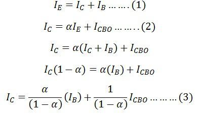
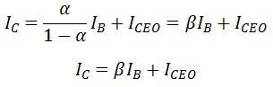
Collector Current
In CE configuration, the input current IB and the output current IC are related by the equation shown below.
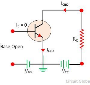
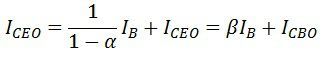
If the base current is open (i.e., IB = 0). The collector current is current to the emitter, and this current is abbreviated as ICEO that means collector- emitter current with the base open.
Substitute the value ΔIB in equations (1), we get,
Characteristics of Common emitter (CE) Configuration
The characteristic of the common emitter transistor circuit is shown in the figure below. The base to emitter voltage varies by adjusting the potentiometer R1. And the collector to emitter voltage varied by adjusting the potentiometer R2. For the various setting, the current and voltage are taken from the milliammeters and voltmeter. On the basis of these readings, the input and output curve plotted on the curve.
Input Characteristic Curve
The curve plotted between base current IB and the base-emitter voltage VEB is called Input characteristics curve. For drawing the input characteristic the reading of base currents is taken through the ammeter on emitter voltage VBE at constant collector-emitter current. The curve for different value of collector-base current is shown in the figure below.
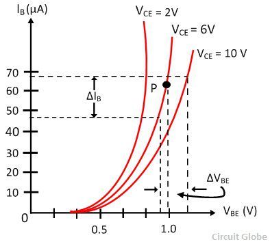
The curve for common base configuration is similar to a forward diode characteristic. The base current IB increases with the increases in the emitter-base voltage VBE. Thus the input resistance of the CE configuration is comparatively higher that of CB configuration.
The effect of CE does not cause large deviation on the curves, and hence the effect of a change in VCE on the input characteristic is ignored.
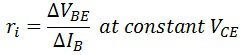
Input Resistance: The ratio of change in base-emitter voltage VBE to the change in base current ∆IB at constant collector-emitter voltage VCE is known as input resistance, i.e.,
Output Characteristic
In CE configuration the curve draws between collector current IC and collector-emitter voltage VCE at a constant base current IB is called output characteristic. The characteristic curve for the typical NPN transistor in CE configuration is shown in the figure below.
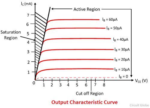
In the active region, the collector current increases slightly as collector-emitter VCE current increases. The slope of the curve is quite more than the output characteristic of CB configuration. The output resistance of the common base connection is more than that of CE connection.
The value of the collector current IC increases with the increase in VCE at constant voltage IB, the value β of also increases.
When the VCE falls, the IC also decreases rapidly. The collector-base junction of the transistor always in forward bias and work saturate. In the saturation region, the collector current becomes independent and free from the input current IB
In the active region IC = βIB, a small current IC is not zero, and it is equal to reverse leakage current ICEO.
Output Resistance: The ratio of the variation in collector-emitter voltage to the collector-emitter current is known at collector currents at a constant base current IB is called output resistance ro.
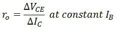
The value of output resistance of CE configuration is more than that of CB
nice article and good representation
good
Nice material for gaining knowledge.
The content is quite beneficial!!
Easy to understand
A short and clear description 😍
This part of electronics was really difficult for me, but this website helped me so much
Nice answer