Definition: A heavily doped semiconductor diode which is designed to operate in reverse direction is known as the Zener diode. In other words, the diode which is specially designed for optimising the breakdown region is known as the Zener diode.
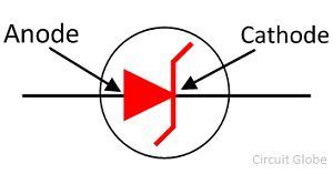
The symbolic representation of Zener diode is shown in the figure below.
Zener Diode Circuit Diagram
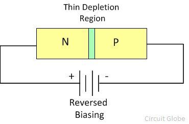
The circuit diagram of the Zener diode is shown in the figure below. The Zener diode is employed in reverse biasing. The reverse biasing means the n-type material of the diode is connected to the positive terminal of the supply and the P-type material is connected to the negative terminal of the supply. The depletion region of the diode is very thin because it is made of the heavily doped semiconductor material.
Working of Zener Diode
The Zener diode is made up of heavily doped semiconductor material. The heavily doped means the high-level impurities is added to the material for making it more conductive. The depletion region of the Zener diode is very thin because of the impurities. The heavily doping material increases the intensity of the electric field across the depletion region of the Zener diode even for the small reverse voltage.
When no biasing is applied across the Zener diode, the electrons remains in the valence band of the p-type material and no current flow through the diode. The band in which the valence electrons (outermost orbit electron) place is known as the valence band electron. The electrons of the valence band easily move from one band to another when the external energy is applied across it.
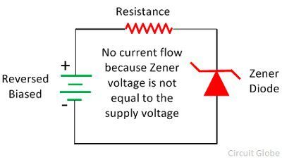
When the reverse bias applies across the diode and the supply voltage is equal to the Zener voltage then it starts conducting in the reverse bias direction. The Zener voltage is the voltage at which the depletion region completely vanish.

The reverse bias applies across the diode increases the intensity of electric field across the depletion region. Thus, it allows the electrons to move from the valence band of P-type material to the conduction band of N-type material. This transferring of valence band electrons to the conduction band reduces the barrier between the p and n-type material. When the depletion region become completely vanish the diode starts conducting in the reverse biased.
Characteristic of Zener Diode
The VI characteristic graph of the Zener diode is shown in the figure below. This curve shows that the Zener diode, when connected in forwarding bias, behaves like an ordinary diode. But when the reverse voltage applies across it and the reverse voltage rises beyond the predetermined rating, the Zener breakdown occurs in the diode.
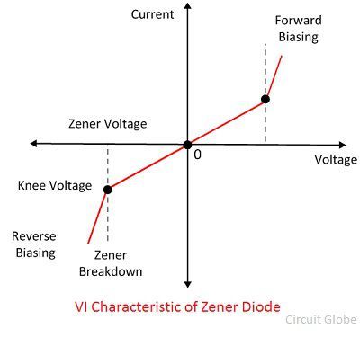
At Zener breakdown voltage the current starts flowing in the reverse direction. The graph of the Zener breakdown is not exactly vertical shown above which shows that the Zener diode has resistance. The voltage across the Zener is represented by the equation shown below.
V = VZ + IZRZ
Applications of Zener Diode
The Zener diode is mostly used in the commercial and industrial applications. The following are the main application of the Zener diode.
As Voltage Stabilizer – The Zener diode is used for regulating the voltage. It provides the constant voltage from the fluctuating voltage source to the load. The Zener diode is connected in parallel across the load and maintain the constant voltage VZ and hence stabilises the voltage.
For Meter Protection – The Zener diode is generally used in multimeters for controlling the movement of the meter against accidental overloads. It is connected in parallel with the diode. When the overload occurs across the diode most of the current pass through the diode. Thus, protects the meter from damage.
For Wave Shaping – The Zener diode is used for converting the sine wave into the square wave.This can be done by placing the two Zener Diodes in series with the resistance. The diode is connected back to back and in the opposite direction.
When the voltage applied across the terminal is less than the Zener voltage the diodes offer a high resistive path to the current and the input voltage applied across a diode appeared at the output terminal. When the voltage rises beyond the Zener voltage they offer a low resistance path and large current flow through the diode. Due to which the heavy voltage drop occurs across the resistance and the input wave cutoff at the peak. Thus, the square wave appears across the output terminal