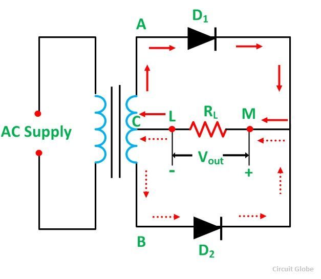
The Center Tapped Full Wave Rectifier employs a transformer with the secondary winding AB tapped at the centre point C. It converts the AC input voltage into DC voltage. The two diode D1, and D2 are connected in the circuit as shown in the circuit diagram below.
Contents:
- Operation of the Center Tapped Full Wave Rectifier
- Peak Inverse Voltage of Center Tapped Full Wave Rectifier
- Video
- Advantages and Disadvantages of Center Tapped Full Wave Rectifier
Each diode uses a one-half cycle of the input AC voltage. The diode D1 utilizes the AC voltage appearing across the upper half (AC) of the secondary winding for rectification. The diode D2 uses the lower half (CB) of the secondary winding.
Operation of the Center Tapped Full Wave Rectifier
When AC supply is switched ON the alternating voltage, Vin appears across the terminals AB of the secondary winding of the transformer. During the positive half cycle of the secondary voltage, end A becomes positive, and end B becomes negative. Thus, the diode D1 becomes forward biased, and diode D2 becomes reverse biased.
The two diodes conduct simultaneously. Therefore, when the diode D1 conducts, the diode D2 does not conduct and vice versa.
When the Diode D1 is conducting, the current (i) flows through the diode D1 load resistor RL (from M to L) and the upper half of the secondary winding as shown in the circuit diagram marked by the red color arrowheads. During the negative half-cycle, the end B becomes positive, and end A becomes negative. This makes the diode D2 forward biased, and diode D1 reverse biased.
When the diode D2 conducts while the diode D1 does not. The current (i) flows through the diode D2 load resistor RL (from M to L) and the lower half of the secondary winding as shown by the red dotted arrows.
The current flowing through the load resistor RL is in the same direction (i.e., from M to L) during both the positive as well as the negative half cycle of the input. Hence, the DC output voltage (Vout = i RL) is obtained across the load resistor.
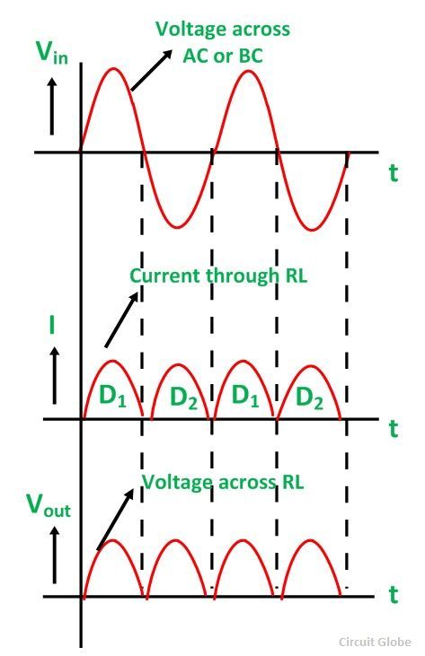
The wave diagram of the input voltage, the current flowing through the load, and the output voltage developed across the load is shown in the figure below:
Peak Inverse Voltage of Center Tapped Full Wave Rectifier
The circuit diagram given below shows the instant when the secondary voltage attains its maximum positive value.
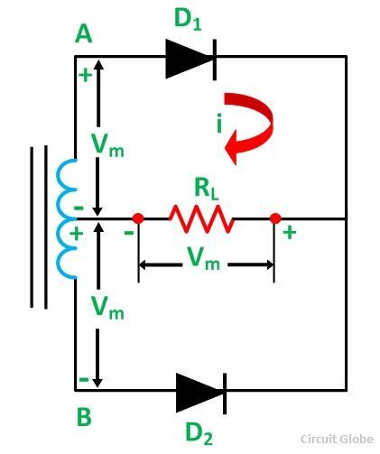
At this instant, Vm developed in the upper half of the secondary winding of the transformer will forward bias the diode D1. This diode conducts, and the current flows through RL, developing Vm voltage across it.
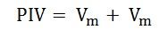
The diode D2 at this instant is reverse biased, and the voltage was coming across it is the sum of the maximum value of voltage developed by the lower half of the secondary winding and the voltage developed across the load. Hence, the peak inverse voltage across the diode D2 is 2Vm.
Video: Full Wave Rectifier
Advantages and Disadvantages of Center Tapped Full Wave Rectifier
- The main advantage is that the output and efficiency are high because an AC supply delivers power during both half cycles.
The Disadvantages of the Center tapped full wave rectifier are as follows:-
- Each diode utilizes only one-half of the voltage developed in the transformer secondary, and thus the DC output obtained is small.
- It is difficult to locate the center on the secondary for the tapping.
- The diode used must be capable of bearing high peak inverse voltage. Because the peak inverse voltage coming across each diode is twice the maximum voltage across the half of the secondary winding.
Thanks
thank you